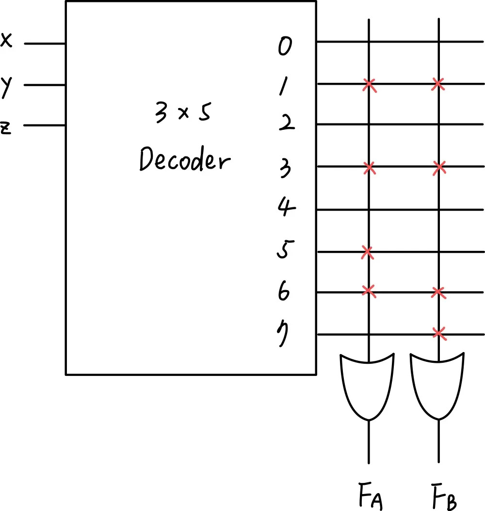
Read Only Memory (ROM)#
Store permanent binary informantion.
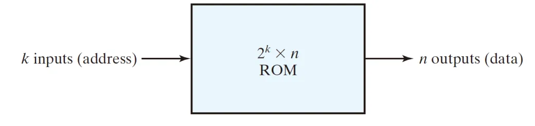
ROM#
Info:
- address input lines
- enables input(s)
- outputs
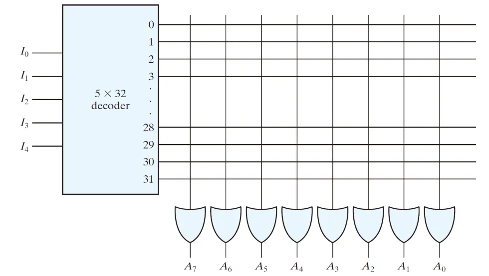
Example : ROM#
- We need to a -to- decoder.
- OR gates (each has inputs).
- programmable interconnections.
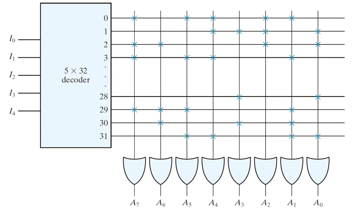
Programmable interconnections#
There are two state:
- Close (two lines are connected)
- Open
A fuse that can be blown by applying a high voltage pluse.
Combinational Circuit Implementation with ROM#
We know basically ROM is decoder and or gates, so …
- It is sum of minterms!
- A boolean function is a sum of minterms!
Hence, we can implement combinational circuit!
For input, output combinational circuit, we need ROM.
Design procedure#
Info:
- Step 1 : Determine the size of ROM
- Step 2 : Obtain the programming truth table of the ROM
- Step 3 : The truth table = the fuse pattern
Example#
Success:
Implement this truth table with ROM:
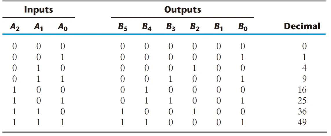
First, we know there is three inputs and 6 outputs, so we need a ROM.
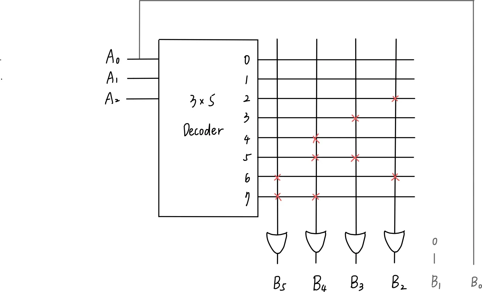
But we can see that and can be simply done without ROM, so we can reduce the ROM to ROM.
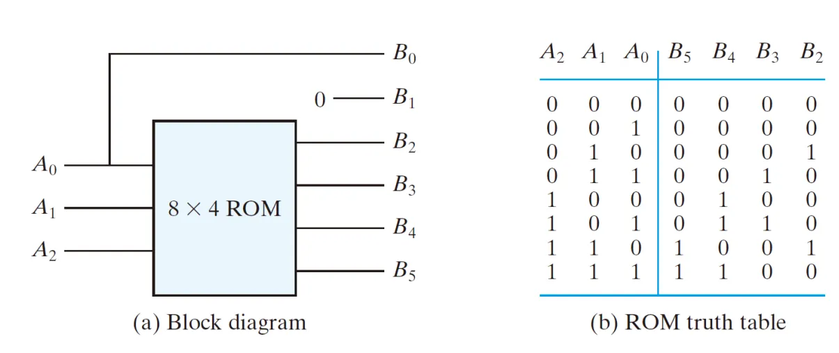 Then now the pattern of truth table will be the fuse pattern :
Types of ROM#
mask programming ROM#
- IC manufacturers
- Is economical only if large quantities
PROM : Programmable ROM#
- Fuses
- Universal programmer
EPROM : Erasable PROM#
- Floating gate
- Ultraviolet light erasable
EEPROM : Electrically Erasable PROM#
- Longer time is needed to write
- Flash ROM
- Limited times of write operations
Programmable two-level logic#
An AND array and an OR array.
There are three types :
Programmable Read-Only Memory (PROM)#

Programmable Array Logic (PAL)#

Programmable Logic Array (PLA)#

We can see that PLA has more flexible than ROM and use less circuits than ROM, so will discuss more about PLA.
PLA#
- An array of programmable AND gates which can generate any product terms of the inputs.
- An array of programmable OR gates which can generate the sums of the products.
Size#
- The number of inputs
- The number of product terms (AND gates)
- The number of outputs (OR gates)
Example#
Say we want to implement the two outputs with three inputs, we can implement with PLA like this
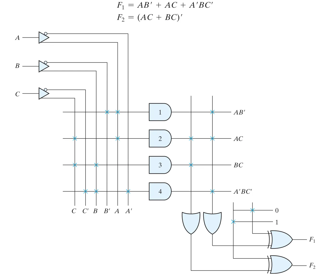
And here is the table :
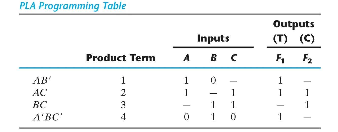 Notice that and the end of the circuit, it use XOR gate to replace invertion gate.
Combinational Circuit Implementation with PLA#
Info:
- Reduce the number of distinct product terms.
- The number of terms in a product is not important.
Example#
Success:
Implement the two functions with PLA :
First, we should draw K-map :
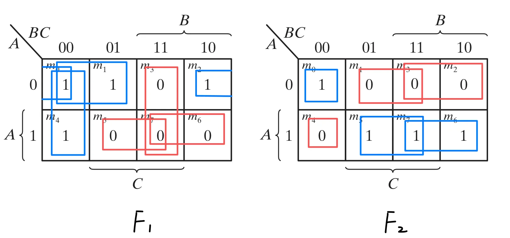
We can see that there are two ways to implement each function :
We can see that there are four possible ways to implement, and different ways may have different number of distinct product terms :
| \ | ||
|---|---|---|
We can see that the combination of has least number of distinct product terms ( terms).
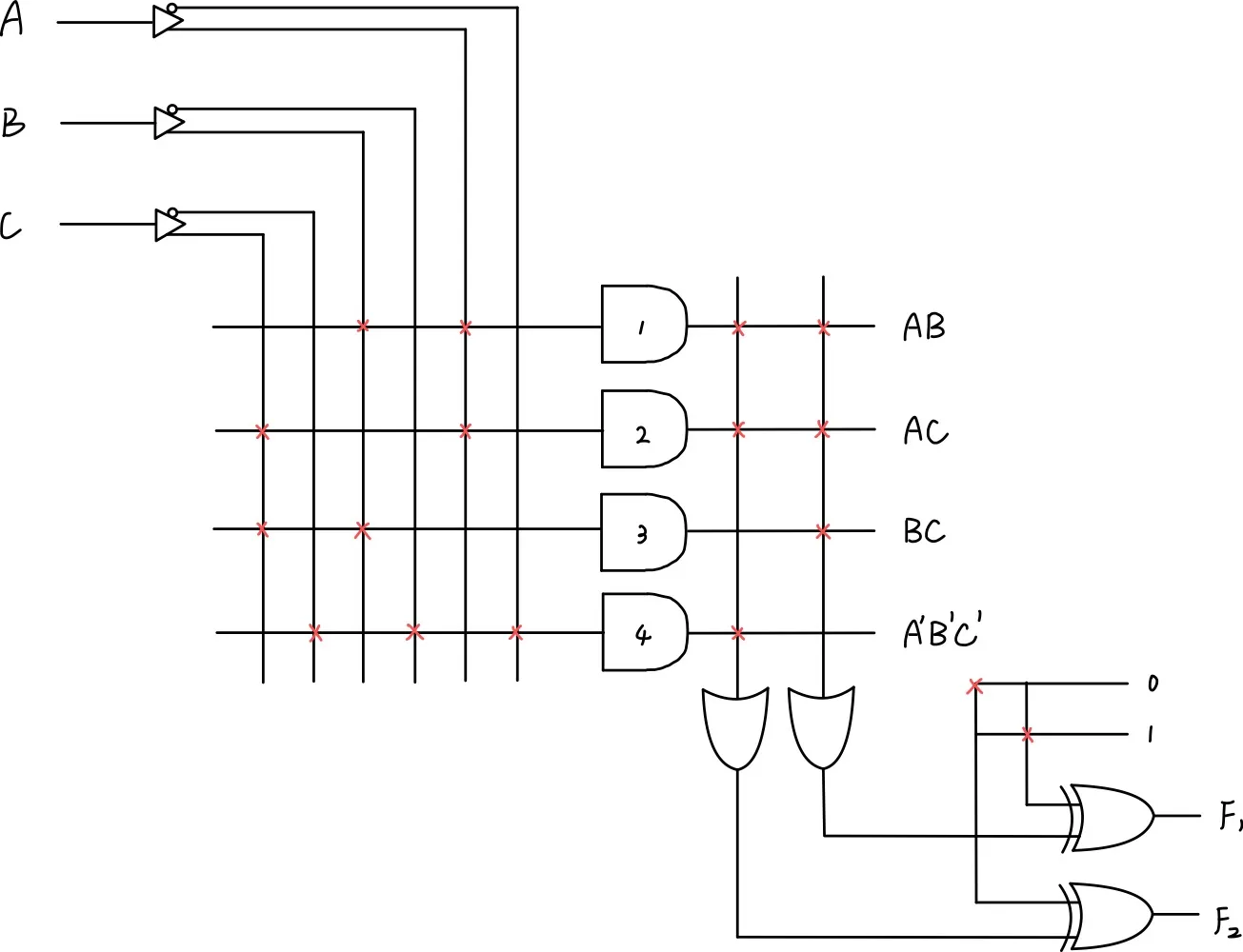
So we will implement in that way, thus we can have the table and the circuit :
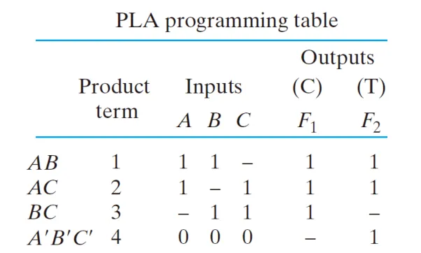
And here is the circuit :
Exercise#
Success:
Tabulate the PLA programming table and the truth table for an ROM for the two Boolean functions listed below.
After tabulating, construct the each circuit diagram.
PLA#
Tabulate:
First, we need to draw K map :
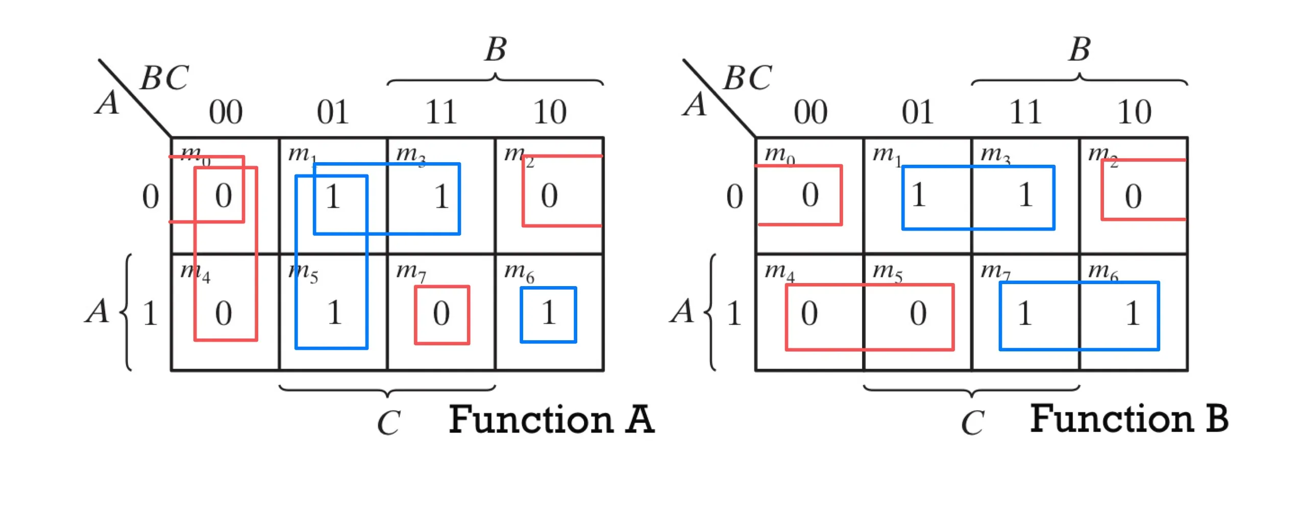
Thus, we can use same strategy above to find the combiantion that has minimum distinct product terms :
| \ | ||
|---|---|---|
There are two possible ways, but for simplicity, we choose .
Then we can tabulate the programming table :
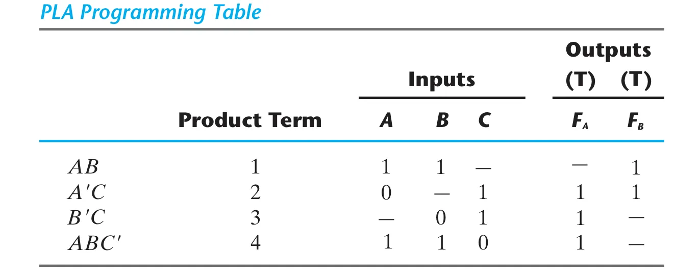
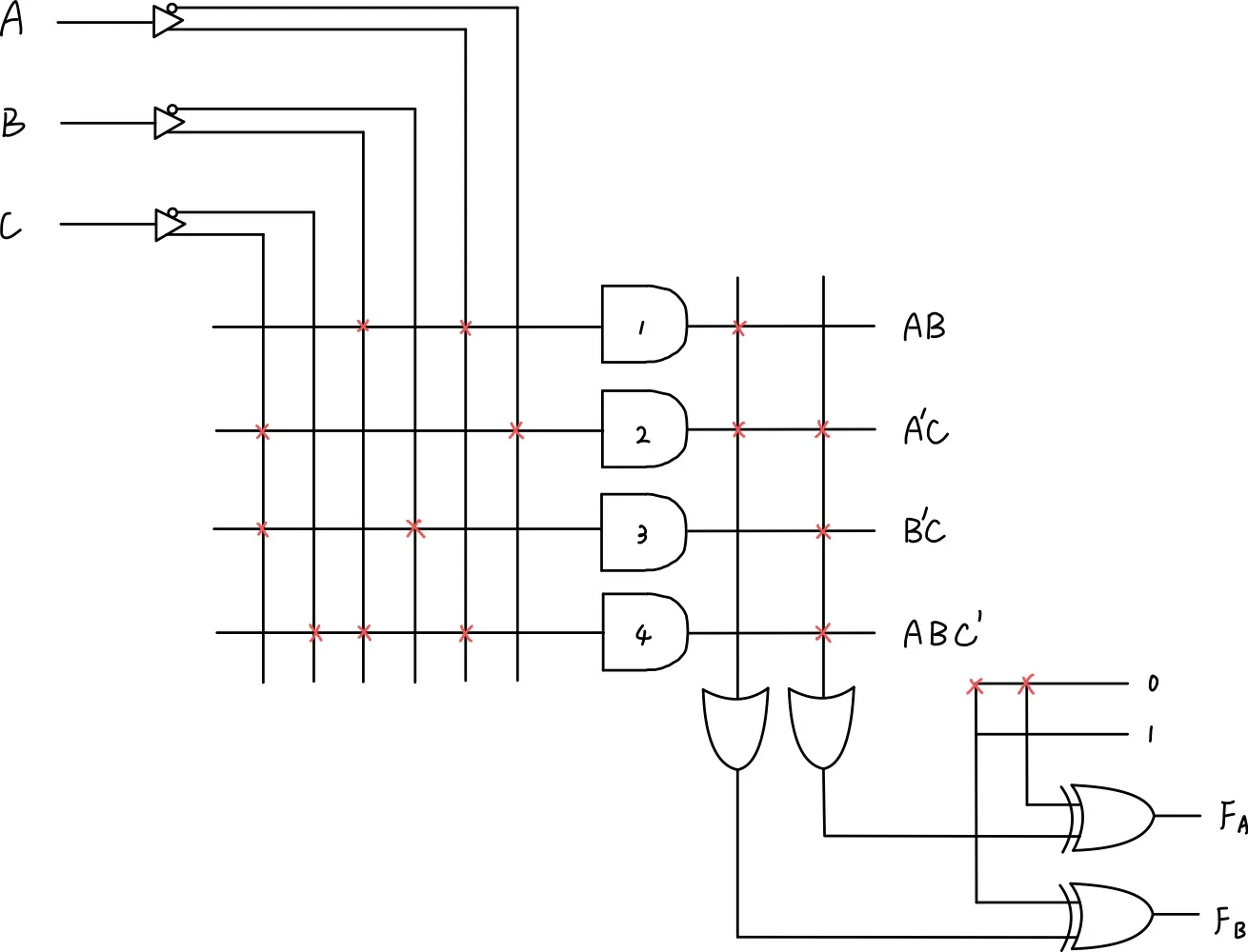
Circuit:
Just use programming table to draw :
ROM#
Tabulate:
It is easy to construct a truth table :
Circuit:
Then use the truth table above, we can simply sketch the circuit :