Analyze and Design Sequential circuit#
Sensitivity List#
- Once using sensitivity list (posedge, negedge), then all signal must use sensitivity list.
- assign use <=. (In sequential circuit
always @(posedge clk), rather than use =. (in combinational circuitalways @*)
| <= | = | |
|---|---|---|
| Using timing | Sequential circuit | Combinational circuit |
| Meaning | Use old value | Use new value |
| Example | 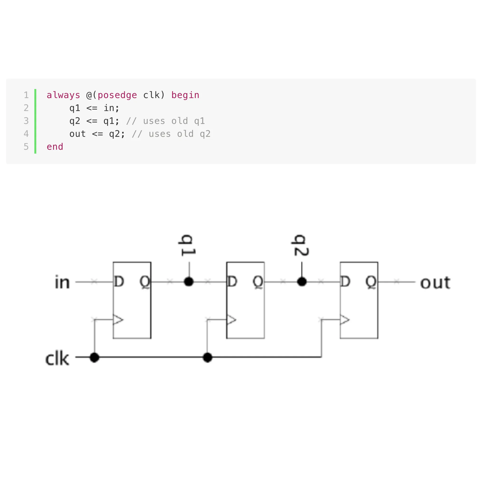 | 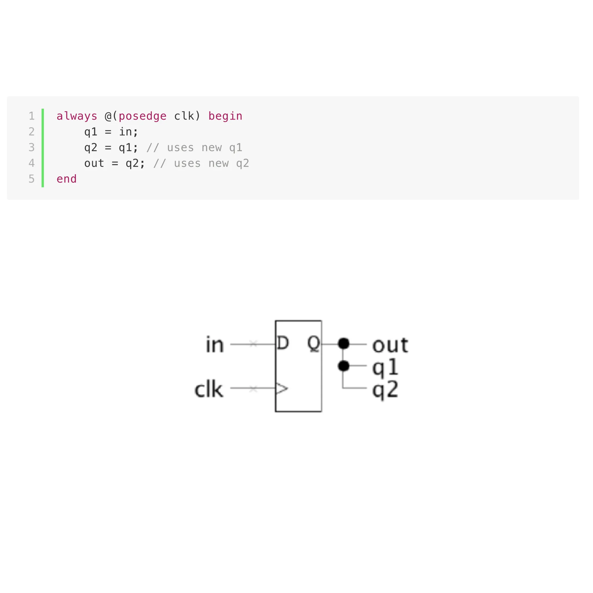 |
- Results of operators (at the left side of assignment) inside always block must be declared as register, for example:
// Code A
reg z;
wire c;
always @* begin
    z = x || y
    c = x || y // wrong code
end

// Code B
wire z;
assign z = x && y // z is not a reg here- There are two types of coding:
// Style 1 : Combinational circuit and sequential circuit are seperate
reg [3:0] count1, next_count1;
always @(posedge clk) // Sequnetial part
    count1 <= next_count1;
always @* begin // Combinational part
    if (reset)
        next_count1 = 0;
    else
        next_count1 = (count1 == 4) ? 0 : count1 + 1;
end
assign enable1 = (count1 == 4);

// Style 2 : Combinational circuit and sequential curcuit are together
reg [3:0] count2;
always @(posedge clk) begin
    if (reset)
        count2 <= 0;
    else
        count2 <= (count2 == 4) ? 0 : count2 + 1;
end
assign enable2 = (count2 == 4);Finite-State Machine (FSM)#
- Sychronous sequential circuit (a.k.a. clocked sequential circuit) is a kind of Finite-State Machine.
- Current state at time is stored in a set of flip-flops.
- (input, current state) => (output, next state) next state at time is a boolean function of the present state and input.
Different types of output function decides different types of circuit.
Mealy machine (circuit)#
Info:
The output is a function of both present state and input.
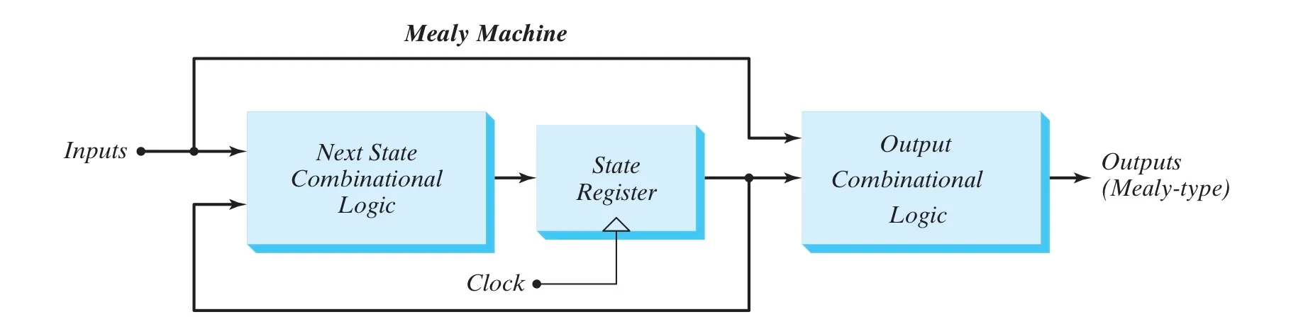 And here is an example state diagram:
digraph mealy{
    layout = circo
    node [shape = circle];
    s1 -> s1 [label = "1/1"];
    s1 -> s2 [label = "0/1"];
    s0 -> s1 [label = "1/0"];
    s0 -> s2 [label = "0/0"];
}Moore machine (circuit)#
Info:
The output is a function of present state only.
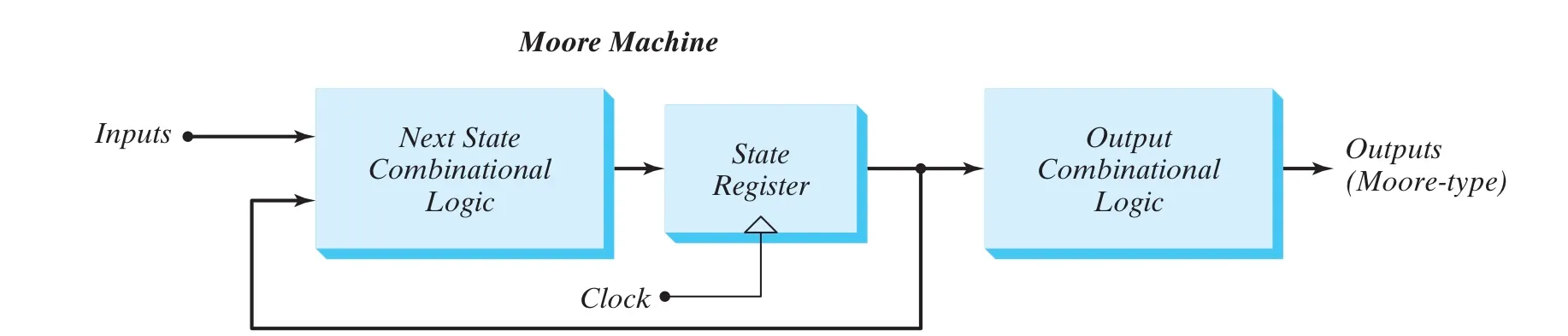 And here is an example state diagram:
digraph moore{
    layout = circo
    node [shape = circle];
    k [shape = point];
    s0 [label = "s0\n 00"];
    s1 [label = "s1\n 01"];
    s2 [label = "s2\n 11"];
    k -> s0 ;
    s1 -> s1 [label = "1"];
    s1 -> s2 [label = "0"];
    s0 -> s1 [label = "1"];
    s0 -> s2 [label = "0"];
}Analysis#
Illustration#
Ok, lets start analyzing.
First, take a look at this example:
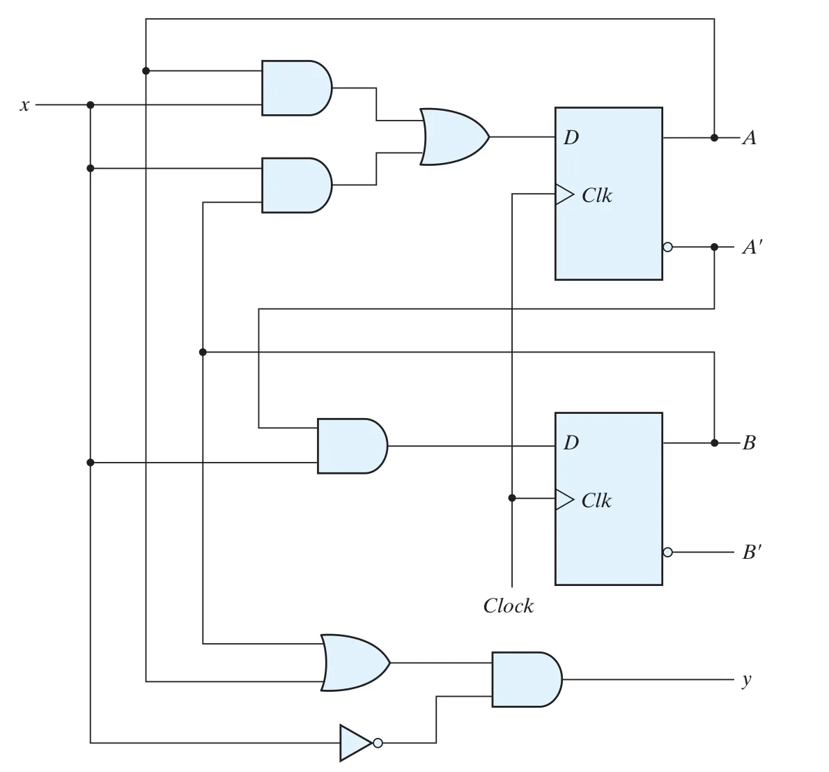 First, look at the combinational part, we can obtain:
process:
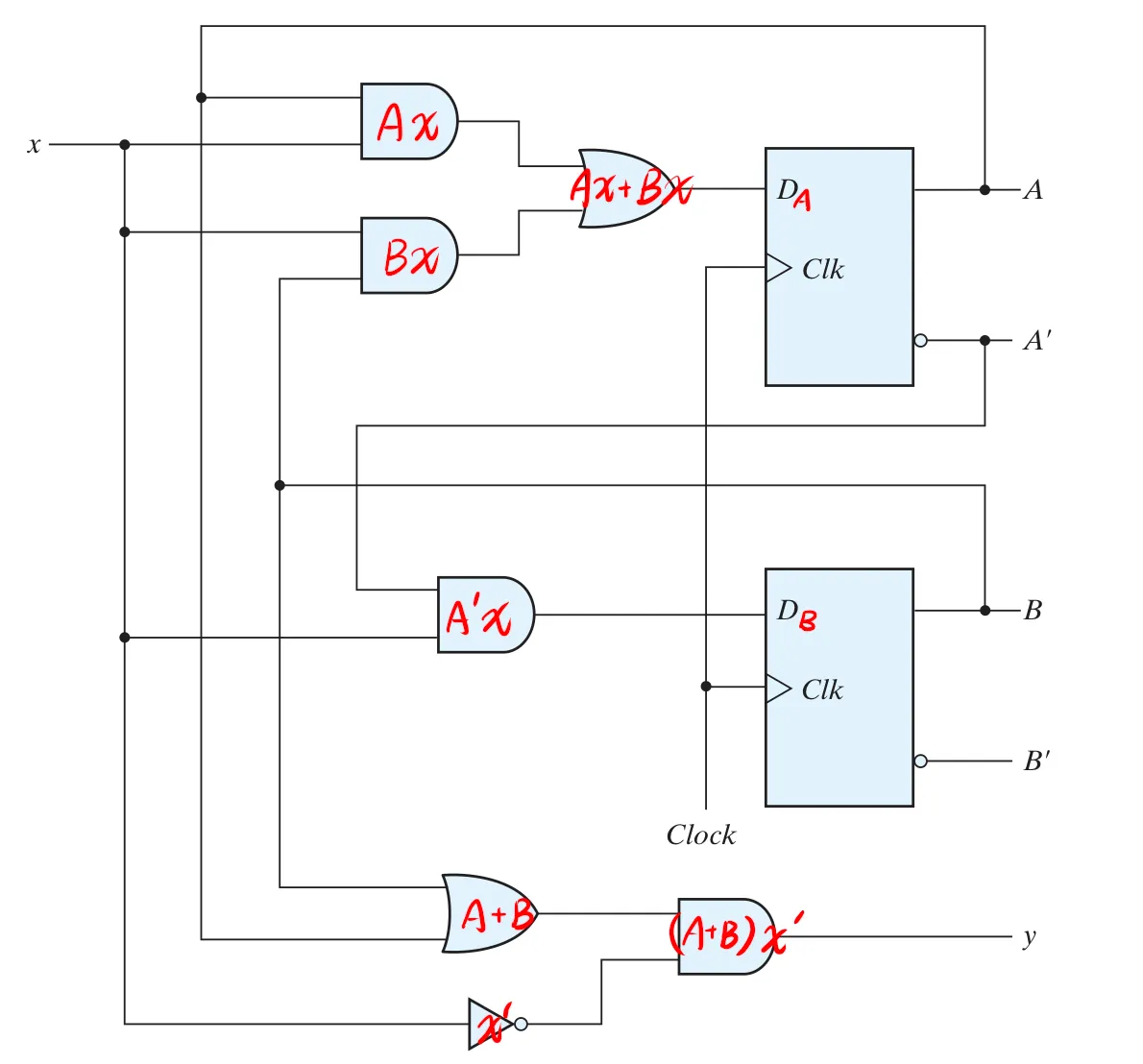
Also, we have known that in a D flip-flop, . So we will get:
Hence, we can get:
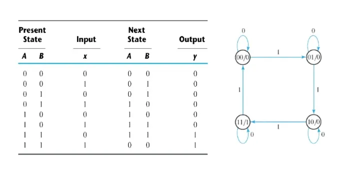
After this process, we want to record the status as truth table,so we define a status table.
There are two ways to represent:
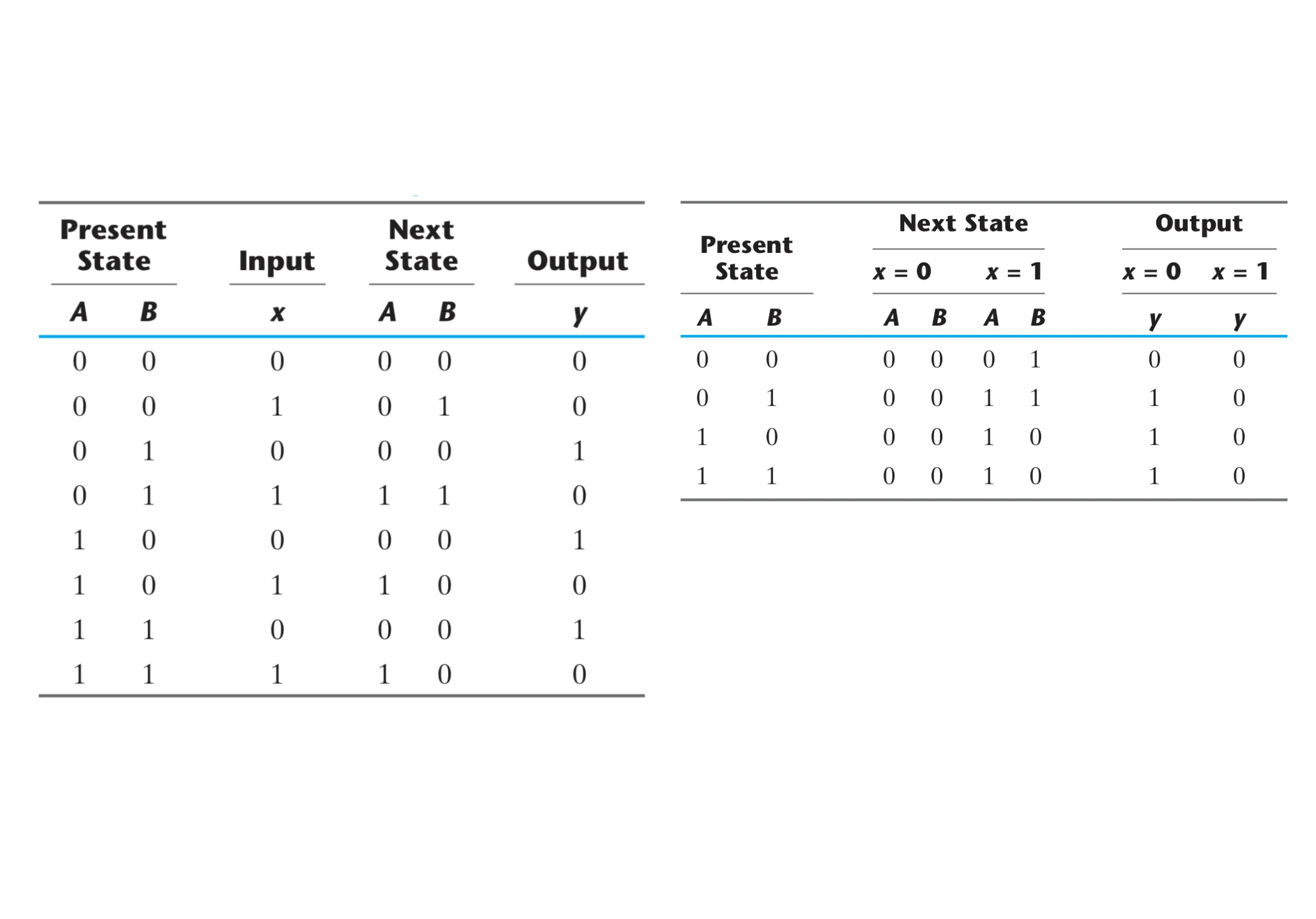 After this, we can use a state diagram to represent the transition.
Info:
After this, we can use a state diagram to represent the transition.
Info:
State diagram#
- circle : a state
- directed line : transition between the states
- On the edge,
it is either
output(Moore) orinput/output(Mealy).
digraph state_diagram{
    node [shape = circle];
    layout = circo;
    00 -> 00 [label = "0/0"];
    10 -> 10 [label = "1/0"];
    00 -> 01 [label = "1/0"];
    01 -> 00 [label = "0/1"];
    01 -> 11 [label = "1/0"];
    11 -> 00 [label = "0/1"];
    11 -> 10 [label = "1/0"];
    10 -> 00[label = "0/1"];

}Now, we can have the step to analyze a sequential circuit:
Lets look at another example.
Example_01 Analyze with DFF#
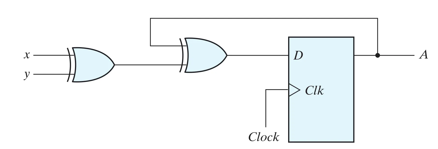 Look at this circuit, we can get:
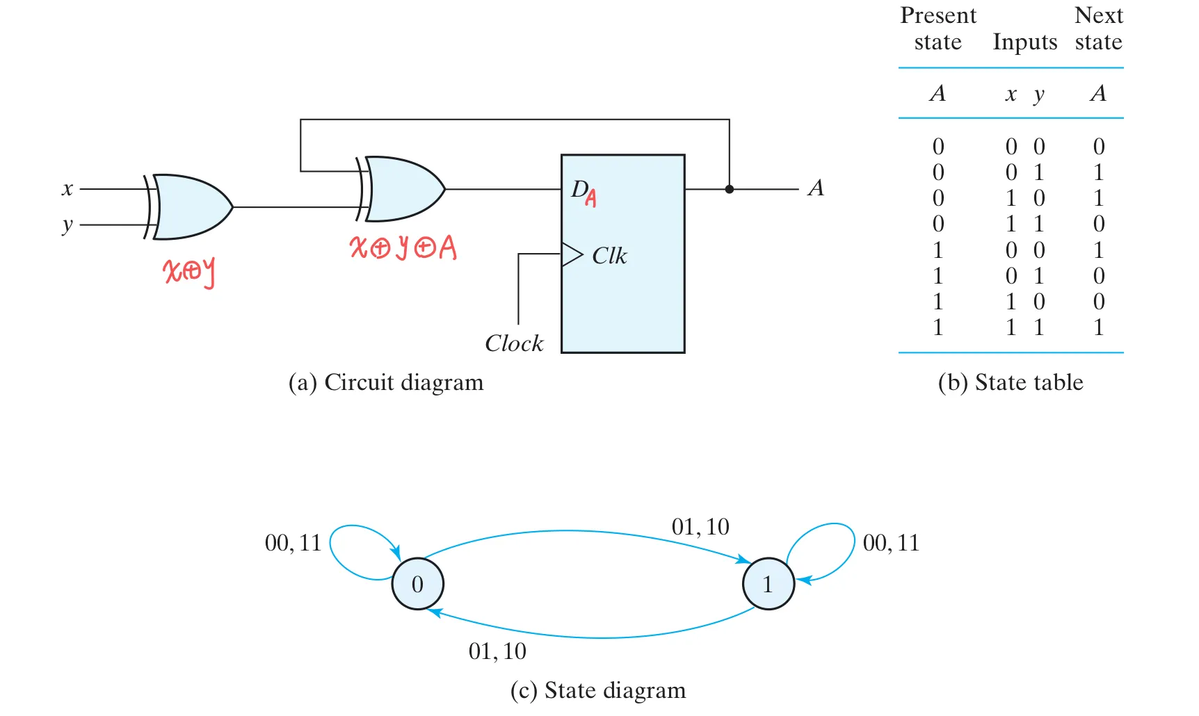
Example_02 Analyze with JKFF#
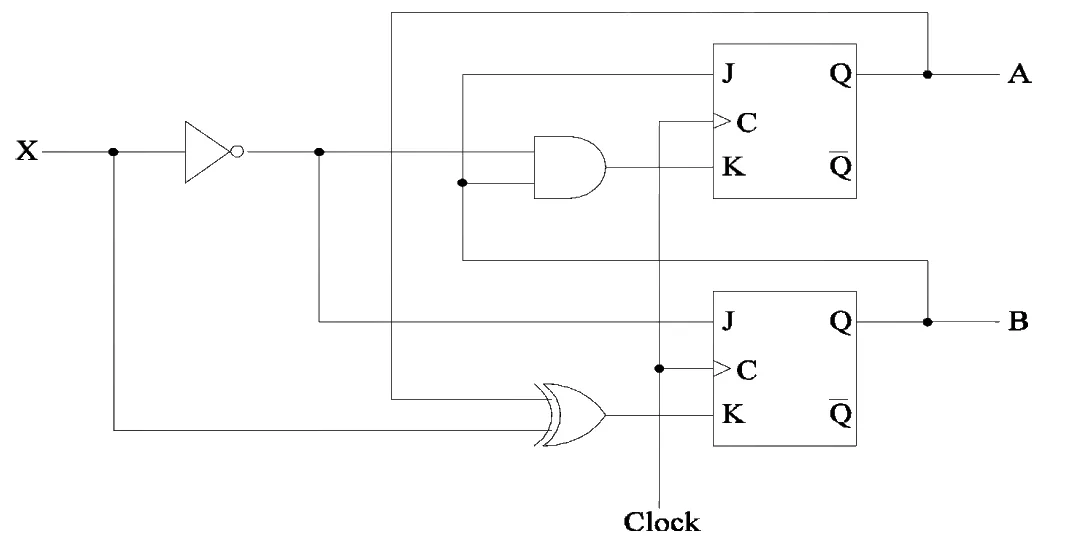 We can find these equations:
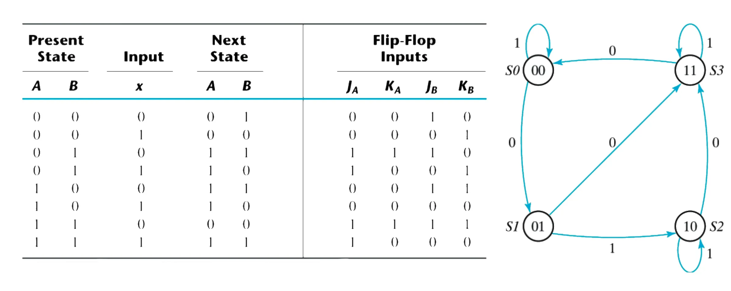
We then apply the characteristic equation :
Complete the state table and diagram:
Example_03 Analyze with TFF#
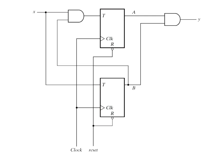 By observation, we can get:
Then by the characteristic equation :
Complete the state table and diagram:
Design#
Illustration#
There is a procedure to produce a sequential circuit: Info:
-
Determine a state diagram or state table.
-
State reduction if necessary.
-
Assign binary values to the states. obtain binary-coded state table
-
Choose the type of flip-flops. derive the simplified flip-flop input equations and output equations
-
Obtain the logic diagram.
Without further ado, lets look at a example.
Example_01 String Detector#
Success:
Illustration#
Construct a recognizer that takes one bit at a time and generates an output when and only when the sequence is detected at the input.
Input#
The input is the continous signal that you need to detect.
Output#
The output is if there is a sequence and otherwise.
Here is an example:
Lets define four states:
- : there is no any char correspond to .
- : so far, we have .
- : so far, we have .
- : so far, we have .
We can design like this:
First, we can construct the straight way to output .
digraph design{
    layout = circo
    node [shape = circle]

    A -> B [label = "1/0"];
    B -> C [label = "1/0"];
    C -> D [label = "0/0"];
    D -> B [label = "1/1"];
}Now, consider those fail condition.
digraph design{
    layout = circo
    node [shape = circle]

    A -> B [label = "1/0"];
    A -> A [label = "0/0", color = red];
    B -> C [label = "1/0"];
    B -> A [label = "0/0", color = red];
    C -> D [label = "0/0"];
    C -> C [label = "1/0", color = red];
    D -> B [label = "1/1"];
    D -> A [label = "0/0", color = red];
}Then we have the state diagram! Here is the corresponding state table:
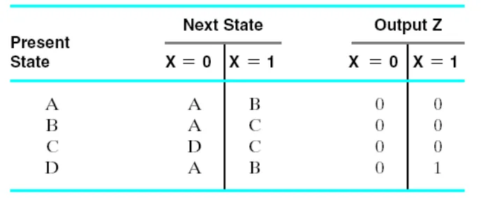
For futher implementation, we need to use binary code to encode those states.
Remember that different binary code assignments may result in different final circuit with different time complexities.
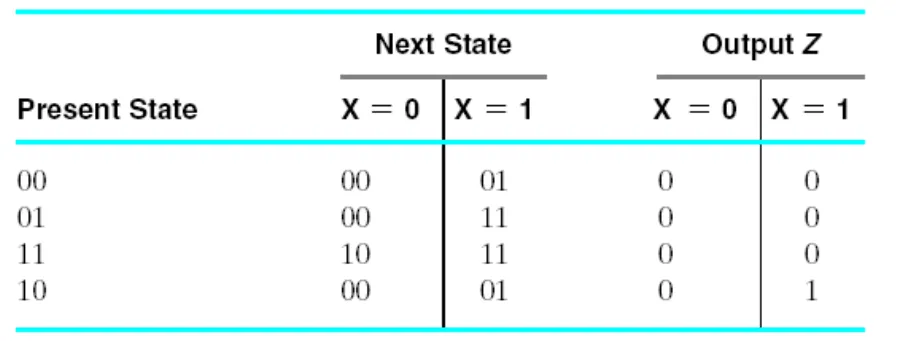
Now, for example, we encode these four states like this, and thus we have:
digraph design{
    layout = circo
    node [shape = circle]
    A [label = "00"];
    B [label = "01"];
    C [label = "11"];
    D [label = "10"];
    A -> B [label = "1/0"];
    A -> A [label = "0/0"];
    B -> C [label = "1/0"];
    B -> A [label = "0/0"];
    C -> D [label = "0/0"];
    C -> C [label = "1/0"];
    D -> B [label = "1/1"];
    D -> A [label = "0/0"];
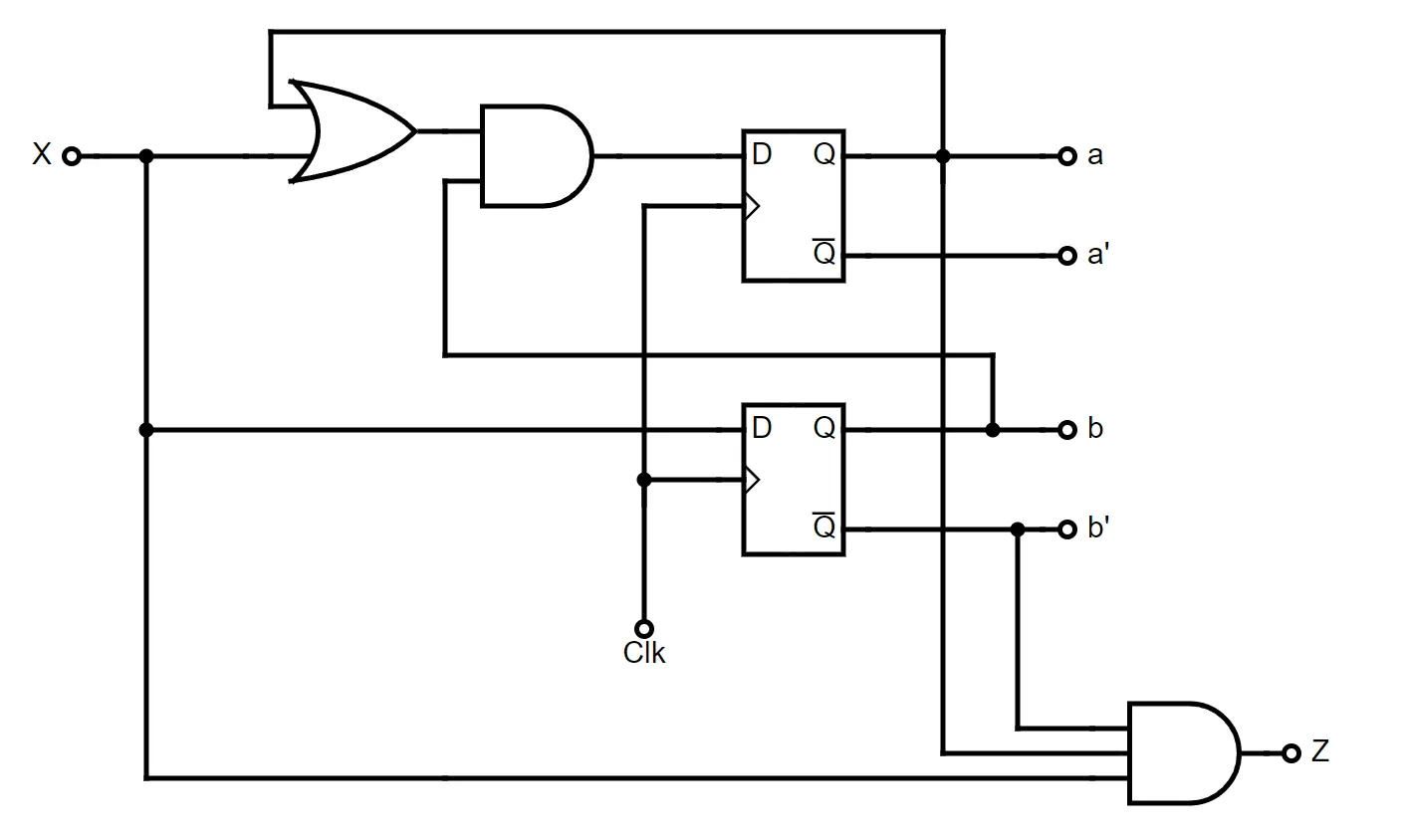
}Now, we are going to implement with D filp-flop. We use to represent the current state (If State is , then ). First, we need to write out the logic equations. details:
By using K-map:
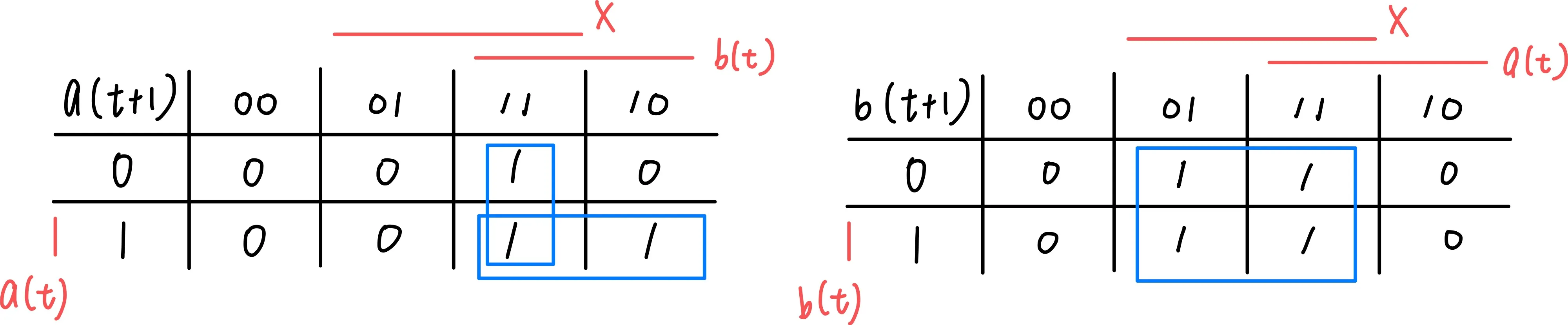 We can have reduced SOP form.
Then by a little reduction on , we can have:
Since we want to use D flip-flop, we can use its characteristic equation to create the storage part.
Hence, we can get the circuit.
Example_02 Vending Machine#
Success:
Illustration#
There are two kinds of coins, one is nickel and one is dime, the relationship is 1 dime = 2 nickels.
Now, design a circuit to determine whether to output a merchandise which price is 3 nickels.
Input#
There are three types of input:
- (Nickel) : insert a nickel.
- (Dime) : insert a dime.
- : back to the initial condition.
Output#
There is one output:
- : 0 is not and 1 is output the merchandise.
First, we can obseve that there are only 5 possible sequence to activate open:
digraph vending{
    rankdir = LR
    node [shape = circle]
    k [shape = point]
    k -> s0 [label = "Reset"];
    s0 -> s1 [label = "N"];
    s0 -> s2 [label = "D"];
    s1 -> s3 [label = "N"];
    s1 -> s4 [label = "D"];
    s3 -> s7 [label = "N"];
    s3 -> s8 [label = "D"];
    s2 -> s5 [label = "N"];
    s2 -> s6 [label = "D"];
    s7, s8, s4, s5, s6 [color = "red"]
}Those states with red color means should output 1, otherwise should output 0.
By State reduction (let every state be the current dollor), we can obtain the state diagram like this:
digraph state{
    rankdir = LR
    node [shape = circle];
    k [shape = point];
    0 [label = "0 Nickel"];
    1 [label = "1 Nickel"];
    2 [label = "2 Nickel"];
    3 [label = "3 Nickel\n [open]", color = "red"];
    k -> 0 [label = "Reset"];
    0 -> 0 [label = "D'N'"];
    0 -> 1 [label = "N"];
    0 -> 2 [label = "D"];
    1 -> 1 [label = "D'N'"];
    1 -> 2 [label = "N"];
    1 -> 3 [label = "D"];
    2 -> 3 [label = "D, N"];
    2 -> 2 [label = "D'N'"];
    3 -> 0 [label = "*"]
}We can encode as follow and get the state table:
| 00 | 0 | 0 | 00 | 0 | 10 | 0 | 0 | 10 | 0 | |
| 00 | 0 | 1 | 01 | 0 | 10 | 0 | 1 | 11 | 0 | |
| 00 | 1 | 0 | 10 | 0 | 10 | 1 | 0 | 11 | 0 | |
| 00 | 1 | 1 | xx | 0 | 10 | 1 | 1 | xx | 0 | |
| 01 | 0 | 0 | 01 | 0 | 11 | 0 | 0 | 00 | 1 | |
| 01 | 0 | 1 | 10 | 0 | 11 | 0 | 1 | 00 | 1 | |
| 01 | 1 | 0 | 11 | 0 | 11 | 1 | 0 | 00 | 1 | |
| 01 | 1 | 1 | xx | 0 | 11 | 1 | 1 | xx | 1 |
Next, obtain the state equations: details:
By K-Map:
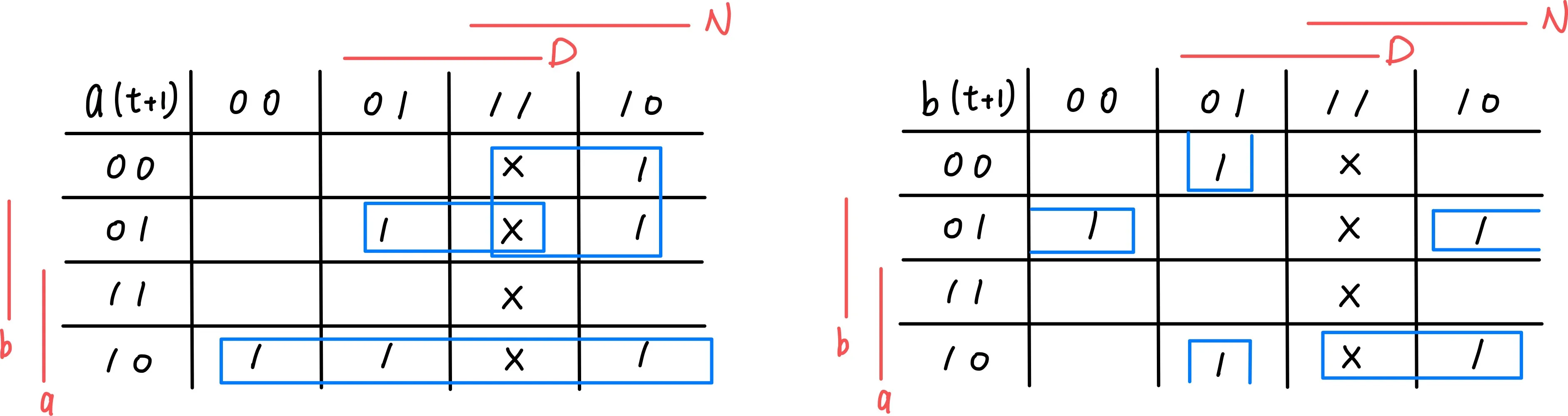 We can have the SOP form:
Using D flip-flop, we can have the characteristic equation $$ \begin{align} D_a &= ab’+Na’+Da’b\ D_b &= DN’b’+D’a’b+Nab’\ Open &= ab \end{align}
Hence, we can get the sequential circuit:  #### Remark In practice, a vending machine’s coin-receptor is a mechanical device and is very slow compared to an electronic circuit․ Inserting a dime (nickel) would cause signal $sense_D$ ($sense_N$) to be asserted for a large number of clock cycles. And there may be an arbitrarily long time between insertion of two consecutive coins․ So, we need to generate a signal such that $D$ ($N$) that will be asserted for 1 clock cycle after $sense_D$ ($sense_N$) becomes 1.  ### Example_03 Circuit w/ JKFF Say we want to implement the following cicuit.  Then we need to derive the table with JK input value:  Remember that $Q(t+1)=JQ'+K'Q$, then we should be able to get this table. Then by k-map, we get the following equations: **K-map:** \begin{align} J_A &= BX’\ K_A &= BX \ J_B &= X \ K_B &= (A \oplus X)’ \ \end{align}
Then we can sketch the circuit.  ### Example_04 N-bit binary counter w/ TFF **Success:** ### Illustration An n-bit binary counter consists of n FFs that can count in binary from $0$ to $2^n-1$. Implement this counter using **TFF**. Here is the state diagram: ```graphviz digraph sta{ node [shape = circle] layout = neato; 000 -> 001 001 -> 010 010 -> 011 011 -> 100 100 -> 101 101 -> 110 110 -> 111 111 -> 000 } ``` Similarly, we need to derive the state table with FF inputs:  Also remember that $Q(t+1)=T\oplus Q$, then the table is quite straight-forward. By k-map: **K-map:** \begin{align} T_{A2} &= A_1A_0 \ T_{A1} &= A_0 \ T_{A0} &= 1 \ \end{align}
Then we can get the circuit:  ### Example_05 Arbiter **Success:** ### Illustration A device asserts its request signal to request for the resource. When the resource is not used, the arbiter selects the highest priority requesting device and asserts its grant signal. When a device finished using the resource, it deasserts its request signal. Implement an arbiter that is for three devices where the priority from high to low is $1\to2\to3$. ### Input Each device provides one input $R$ ( Request ) to the arbiter. ### Output The arbiter provides one output $G$ ( Grant ) for each device. First, we can draw the status diagram like this: ```graphviz digraph arbiter{ node [shape = circle] g1 [label = "G=100"] g2 [label = "G=010"] g3 [label = "G=001"] Idle -> g1 [label = "1xx"] Idle -> Idle [label = "000"] g1 -> g1 [label = "1xx"] g1 -> Idle [label = "0xx"] Idle -> g2 [label = "x1x"] g2 -> g2 [label = "x1x"] g2 -> Idle [label = "x0x"] Idle -> g3 [label = "xx1"] g3 -> g3 [label = "xx1"] g3 -> Idle [label = "xx0"] } ``` Here, rather than drawing the circuit, we use verilog to describe this module: ```verilog= module arbiter (r, Reset, Clock, g); input [1:3] r; // request signals input Reset, Clock; output wire [1:3] g; // grant signals reg [2:1] state, next; parameter Idle = 2'b00, gnt1 = 2'b01, gnt2 = 2'b10, gnt3 = 2'b11; // Sequential block always @(posedge Clock) if (Reset == 1) state <= Idle; else state <= next; // Define output (Decoder) assign g[1] = (state == gnt1); assign g[2] = (state == gnt2); assign g[3] = (state == gnt3); // Next state combinational circuit always @(r, state) case (state) Idle: casex (r) 3'b000: next = Idle; 3'b1xx: next = gnt1; 3'b01x: next = gnt2; 3'b001: next = gnt3; default: next = Idle; endcase gnt1: if (r[1]) next = gnt1; else next = Idle; gnt2: if (r[2]) next = gnt2; else next = Idle; gnt3: if (r[3]) next = gnt3; else next = Idle; default: next = Idle; endcase endmodule ``` ### Verilog code for FSM > There are more than one way to describe a FSM. In the sample code above (Example_05) - 1st always block introduces flip-flops into the circuit - 2nd always block describes the combinational circuit for computing the next state - The outputs are defined with conditional assignment statements - State transition should use non-blocking assignment (`<=`)as FFs of synchronous sequential circuit are updated concurrently by a common clock ### Remark 1. **Heuristic State Assignment Guidelines** - States having the same next state for a given input should be given adjacent assignments. - States that are next states of a single state should be given adjacent assignments. - States having the same output for a given input should be given adjacent assignments. (2 states are adjacent if they differ in one variable) 2. **Unused States** - Unused states can be treated as don’t care conditions to simplify the circuit. - But, for more robust design it may be desirable to specify the next states and/or output values for the unused states upon a malfunction. 3. **Start State/Reset State** - A master reset signal is usually provided for initializing the flip-flop states. 4. **Timing Issues** - External input changes must be properly timed with respect to active edge to ensure correct operation. - Must give enough time for signals to be transmitted to flip-flop inputs before we sample the flip-flop inputs.  ## Optimization ### State Reduction The main idea is to merge the equivalent state. **Info:** Define:Two states of a FSM are equivalent if \the outputs produced for each possible input value are identical\and the next states for each possible input value are the same or equivalent
- Merits of state reduction : Can reduce number of flip-flops used. We use the following example to demonstrate state reduction.  We can see that $g$ and $e$ has the same output and also the same Next state, so we can merge those two status. Then we get:  Here, we obtain new equivalent states $d = f$, so one can do merge again:  ### State Assignment Cost of final circuit depends on the state assignment. There are many possible binary state assignment(encode), for example:  We can see that One-hot encoding uses more FFs (Flip-Flop) but may lead to simpler decoding logic for next state and output. ###### tags: `Logic Design EECS1010`