Random Access Memory (RAM)#
Memory#
Definition#
A collection of storage cells with the necessary circuits to transfer informantion to and from them.
Terminalogy#
- Bit : a single binary digit (0/1).
- Byte : a collection of 8 bits accessed together.
- Word : a collection of bits whose size is a typical unit of access for the memory (machine dependent).
- 1K = , 1M = , 1G = , 1T = .
Memory block diagram#
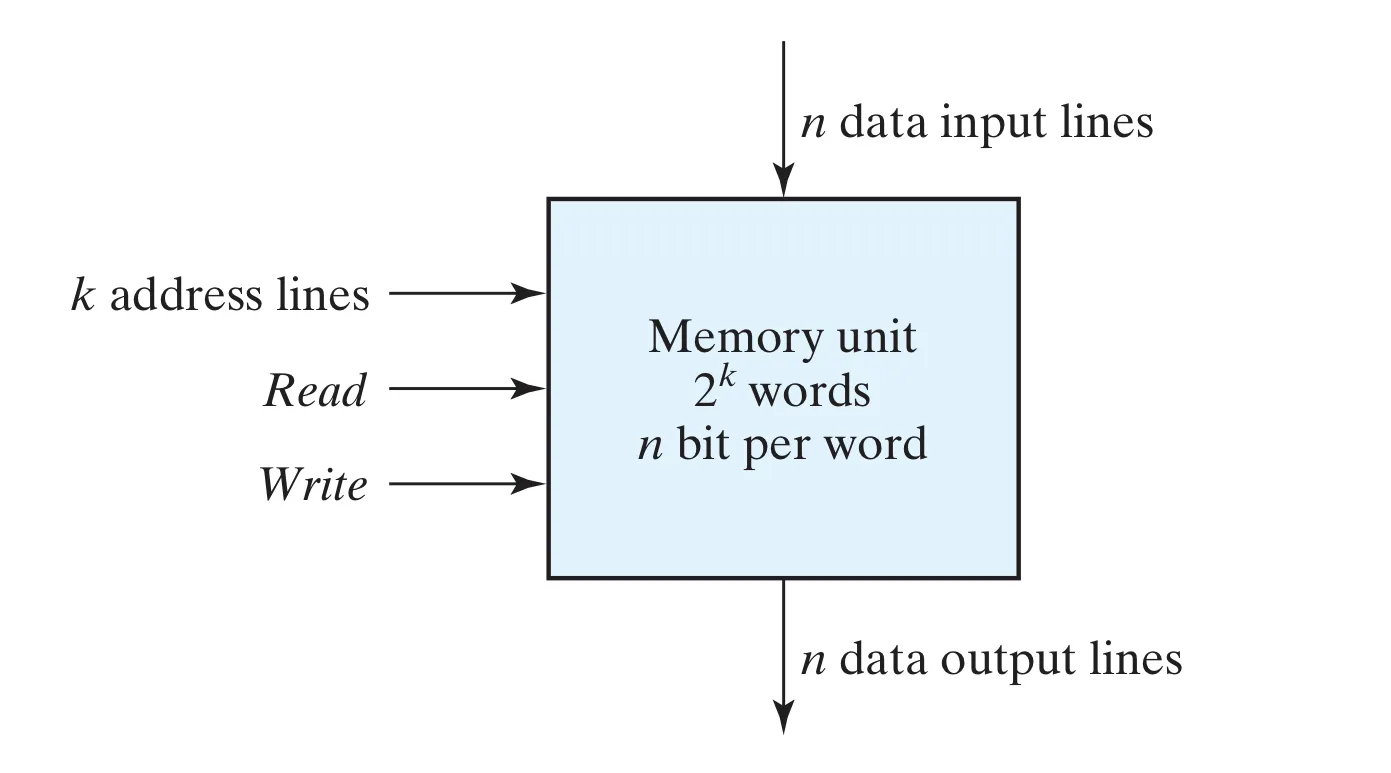 address lines indicates which address we want ( addresses).
indicates the length of the data (word).
Info:
address lines indicates which address we want ( addresses).
indicates the length of the data (word).
Info:
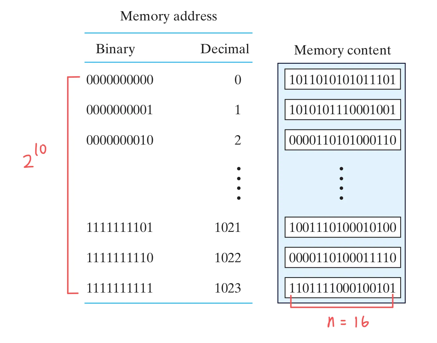
Here is an example of a memory.
Comparison between differnt memory technology#
Here is the ranking :
| Memory Technology | Speed (Fast) | Price (Cheap) |
|---|---|---|
| SRAM | 1 | 4 |
| DRAM | 2 | 3 |
| Magnetic disk | 4 | 1 |
| Flash | 3 | 2 |
Memory Operations#
Write#
Writing into memory a new word.
- Apply the address of the write location to the address lines.
- Place the word to be stored to the data input lines.
- Activate the Write control input.
Write cycle time : maximum time from the application of the address to the completion of all internal memory operations required to store a word.
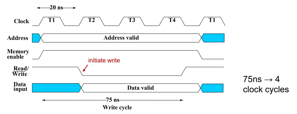
There are some things should be noticed:
- Address must already be ready before changes to 0 to avoid destroying data in other location
- must stay 0 long enough for write operation to complete
- Address must remain stable a short time after goes high to avoid destroying data in other location
Read#
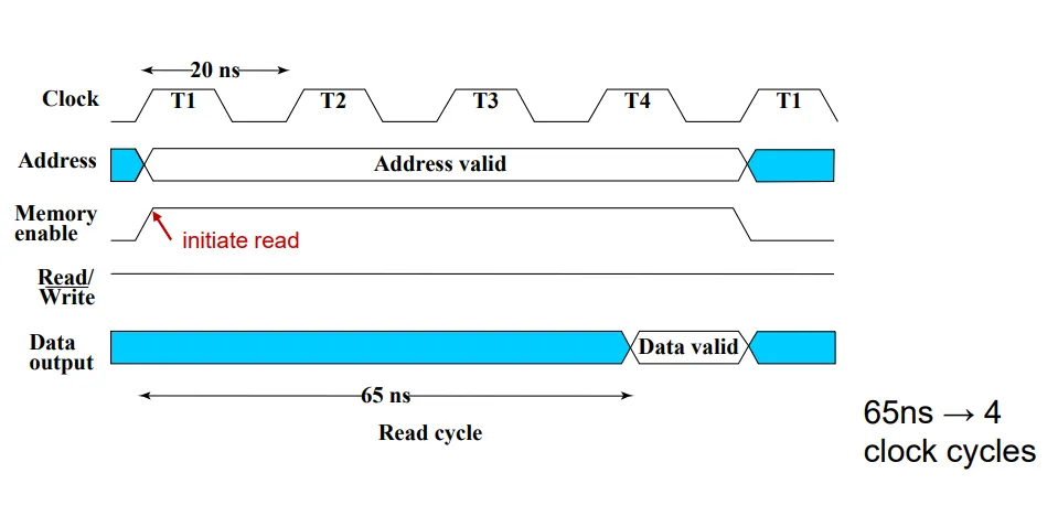
Reading a word from memory.
- Apply the address of the desired word to the address lines.
- Activate the Read control input
Access time : maximum time from the application of the address to the appearance of the data at the data output lines.
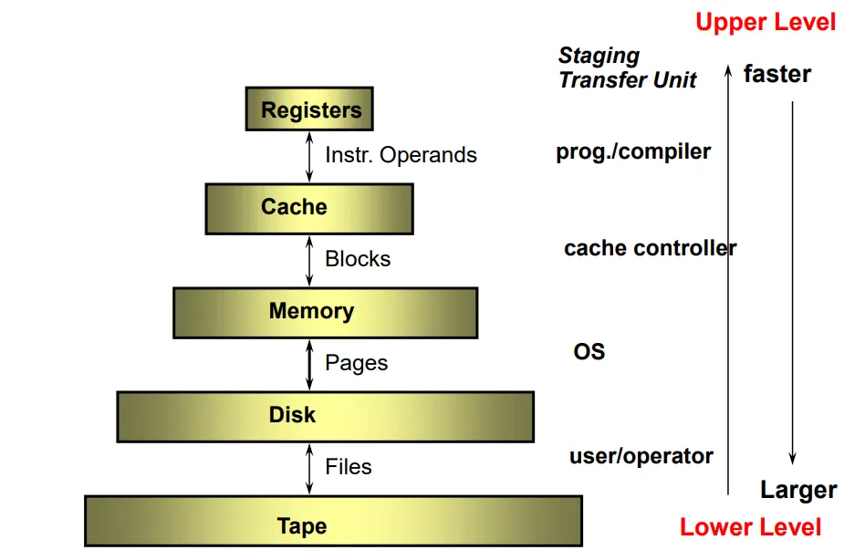
Memory Hierarchy (記憶體階層)#
We try to get a large, fast, and cheap memory.
But in reality, we don’t have such thing.
So we need to try to combine different memories!
Principle#
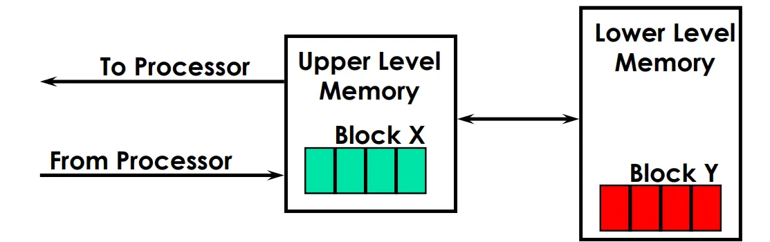
At any given time, data is copied between only two adjacent levels:
- Upper level : the one closer to the processor Smaller, faster, uses more expensive technology
- Lower level : the one away from the processor Bigger, slower, uses less expensive technology
- Block : basic unit of information transfer Minimum unit of information that can either be present or not present in a level of the hierarchy
Locality#
Program access a relatively small portion of the address space at any instant of time.
- 90/10 rule: 10% of code executed 90% of time.
There are two types of locality:
- Temporal locality If an item is referenced, it will tend to be referenced again soon.
- Spatial locality If an item is referenced, items whose addresses are close by tend to be referenced soon.
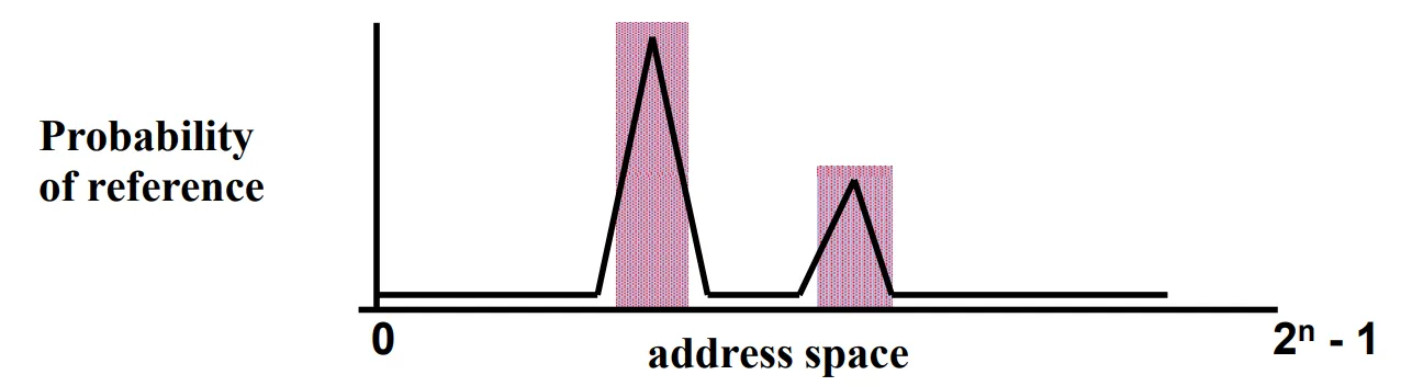
We can see that the adjacent spaces have a higher chance to be referenced.
RAM#
Definition#
- Random-access memory takes the same time to access any word regardless of location.
Contrary, serial memories like tapes and disks which takes different amount of time to access words at different locations.
- Allows both read and write operations.
Types#
| Random Access | S(Static)RAM | D(Dynamic)RAM |
|---|---|---|
| Density | Low | High |
| Power | High | Low |
| Price | High | Low |
| Speed | Fast | Slow |
| Property | Content will last until lose power | Need to be refreshed regularly (Stored in capacitor) |
| Address | Address not divided | Addresses in 2 halves (memory as a 2D matrix) |
| Usage | caches | main memory |
| Implementation | A typical SRAM cell is made up of two inverters plus two pass transistors (Thus a total of 6 transistors) | A typical DRAM cell consists of a capacitor plus one pass transistor |
select (wordline)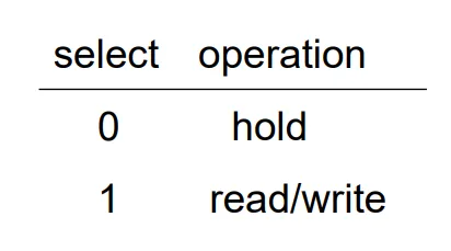 | 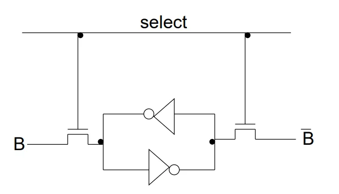 | 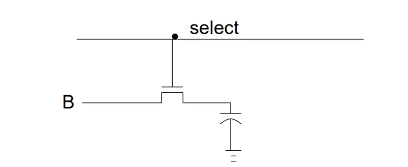 |
Both SRAM and DRAM are volatile memories which lose the stored information when power is turned off.
Nonvolatile memories such as ROM, disk, flash and tape which still retain the stored information when power is off.
RAM Chip#
- RAM bit slice : a set of RAM cells with associated read and write circuits.
A typical RAM chip consists of Info:
- one or more RAM bit slices
- circuit for address decoding
- a three-state buffer for each output line
Here are some examples:
SRAM using a RAM Cell Array#
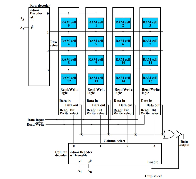
SRAM using a RAM Cell Array#
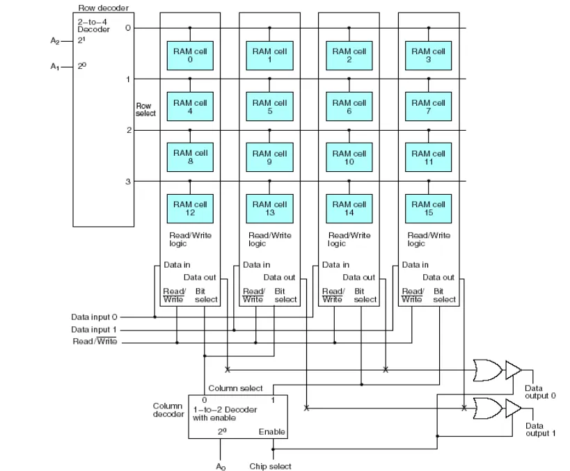
Reuse RAM Chips#
Making wider memory from RAM ICs#
Success:
Construct a RAM using RAM ICs.
Since we want more bits in a word, so we can think as putting two small ICs in parallel.
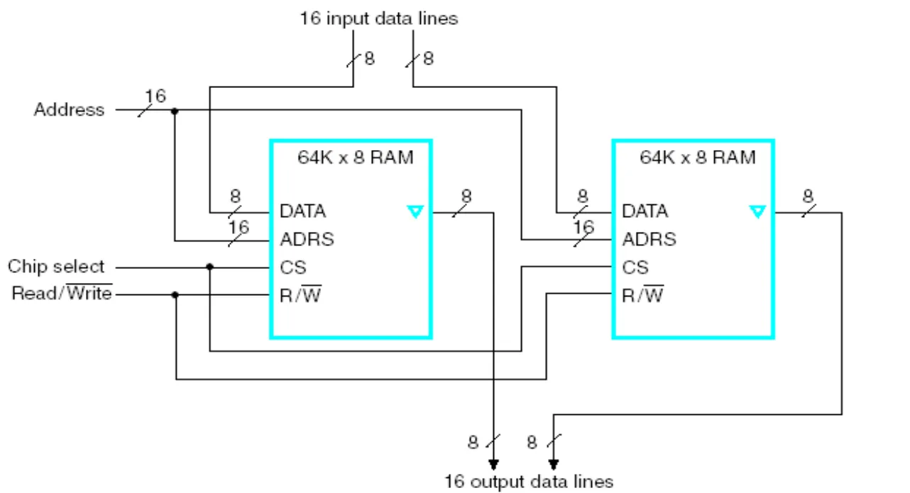
ADRS : ADResS lines CS : Chip Select R/W’ : Read/Write Success:
Construct a RAM using RAM ICs.
Since we want more addresses with the same word size, so we can think as putting 4 small ICs in sequence, and use the first and second ( ) MSB(most significant bit) to determine using which small RAM IC.
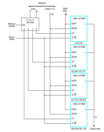
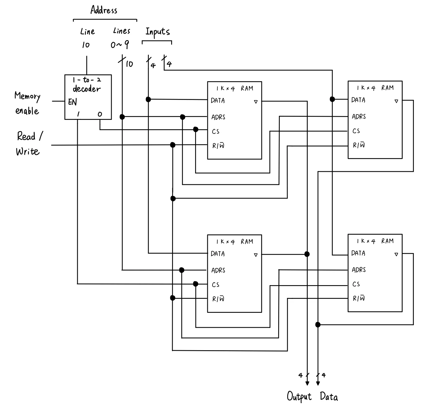
Exercise#
Success:
Construct a RAM using RAM ICs.
Answer: